2. UETRV_Pcore: Design Document
UETRV_Pcore is a RISC-V based application class SoC integrating a 5-stage pipelined processor with memory and peripherals. Currently, the core implements RV32IMAZicsr ISA based on User-level ISA Version 2.0 and Privileged Architecture Version 1.11 supporting M/S/U modes. Following are the key features of the SoC:
2.1. Introduction
2.1.1. Key Features
32-bit RISC-V ISA core that supports base integer (I) and multiplication and division (M), atomic (A) and Zicsr (Z) extensions (RV32IMAZicsr).
Supports user, supervisor and machine mode privilege levels.
Support for instruction / data (writeback) caches.
Sv32 based MMU support and is capable of running Linux.
Cache size, TLB entries etc., are configurable.
Intergated PLIC, CLINT, uart, spi peripherals.
Uses RISOF framework to run architecture compatibility tests.
2.1.2. System Design Overview
The UETRV_Pcore is an applicaion class processor capable of running Linux. A simplified 5-stage pipelined block diagram is shown below. The M-extension is implemented as a coprocessor while memory-management-unit (MMU) module is shared by instruction and data memory (alternatively called load-store-unit (LSU)) interfaces of the pipeline. Specifically, the page-table-walker (PTW) of the MMU is shared and there are separate TLBs (translation look aside buffers) for instruction and data memory interfaces. The A-extension is implemented as part of the LSU module.

The SoC block diagram shows the connectivity of the core with memory sub-system as well as different peripherals using data bus. The boot memory is connected to both instruction and data buses of the core using a bus multiplexer. The instruction and data caches share the main memory using a bus arbiter. Different necessary peripherals are connected using the data bus.

2.1.3. SoC Memory Map
The memory map for the SOC is provided in the following table.
Base Address |
Description |
Attributes |
|---|---|---|
0x8000_0000 |
Memory |
R-X-W |
0x9000_0000 |
UART |
R-W |
0x9400_0000 |
PLIC |
R-W |
0x9C00_0000 |
SPI |
R-W |
0x0200_0000 |
CLINT |
R-W |
0x0000_1000 |
Boot Memory |
R-X |
R: Read accessW: Write accessX: Execute access
2.2. Design Details
The core and SoC design details are outlined in the following subsections.
Instruction fetch and decode stages
Execute stage and M-extension
Memory and writeback stages
Pipeline controller
D-Cache
I-Cache
Memory management unit (MMU) details
Booting and peripherals
UETRV_Pcore is a five stage pipeline which consists of the following stages:
fetch
decode
execute
load store unit(lsu)
writeback
The figure below shows the top module level diagram of pipeline.

2.2.1. Instruction Fetch and Decode Stages
The instruction fetch stage of the pipeline reads instructions either from the boot memory (bmem) or from the instruction cache (icache). The default/reset value of the program counter (PC) starts execution from bmem, which normally contains the zero-order bootloader. After booting, the PC jumps to the main memory region to start user program execution.
If virtual addressing is turned on then both virtual-to-physical address translation (using memory management unit (MMU)) followed by fetching the instructions from icache are performed during fetch stage. Cascading the two key operation can easily make this phase to become crtical path. An instruction page fault exception from the MMU (due to failuare of virtual address translation) gets into the pipeline at fetch stage and propagates till the memory stage before the corresponding exception service routine is called.
The decode stage performs instruction decoding as well as operand fetching from the register-file. The register file write operation is performed on the falling edge of the clock to reduce the hardware cost of full forwarding.
2.2.2. Execute Stage and M-extension
Execute stage implements all the integer ALU operations required by the base RV32I. The forwarding multiplexer is implemented in the execute stage. The input operands to the M-extension are provided by the execute stage, while the result from M-extension is provided to the memory stage. The multiplication instructions are implemented using fast multiplier, while the division and remainder instructions are implemented using a multi-cycle implementation.
2.2.3. Memory and Writeback Stages
Memory stage houses load-store-unit (LSU), control-status-register (CSR) register-file and A-extension. LSU module performs load/store operaions from/to dcache as well as peripheral devices, using data bus. The load/store operations from/to peripheral devices are non-cacheable. The LSU module does not support misaligned accesses. When virtual addressing is enabled LSU module interacts with the MMU module using dedicated request response channel, for address translation. Further details regarding virtual address translation are provided later in MMU module related subsection.
2.2.3.1. A-extension
The execution of A-extension instructions is a multi-cycle operation and leads to pipeline stall. There are two groups of instructions in A-extension. First group comprise of atomic-memory-operation (AMO) instructions while second group involves load-reserved (LR) and store-conditional (SC) instructions.
The AMO instructions involve the following three phases:
Loading one operand from memory
Performing the (requested) operation
Storing the result to memory (at the same address used by load operation in the first phase)
The LR and SC instructions work as a pair. When an LR instruction is executed it requires temporary storage for holding both the address as well as the data. For that purpose we have implemented a single entry buffer that becomes occupied on executing an LR instruction. The buffer remains occupied until a corresponding SC instruction is executed. The buffer is freed irrespective of the fact that SC instruction execution was successful. Using a single entry buffer does not limit the performance, assuming nested LR instructions are not permitted.
2.2.3.2. CSR Module
The memory stage also implements the CSR read/write operations including exception and interrupt handling. The CSR read and write operations are performed in the same cycle. Since the write back stage is never stalled, it is safe to retire CSR and memory write operations in the memory stage (rather writeback/commit stage).
The CSR module is responsible for the implementation of privileged architecture of the RISC V specifications. The module implements M (machine), S (supervisor) and U (user/application) privileged levels.
External interrupts are asynchronous and require synchronization for their precise handling. An approach based on interrupt continuable instruction is followed for percise interrupt handling. For that purpose, the interrupt is put on hold if the pipeline was either stalled or being flushed at the time of occurrence of the interrupt.
2.2.4. Pipeline Controller
Key operations performed by the pipeline controller involve forwarding/stalling/flushing of the pipeline stages. The current version implements full forwarding. LSU operations lead to one stall cycle. In case of load use hazard, forwarding is always performed from the writeback stage and results in an extra stall cycle. Below are some possible scenarios leading to pipeline stalls.
Fetch/decode/execute/memory stages stall due to data TLB miss, dcache miss, executing atomic and other A-extension instructions
Fetch/decode/execute/memory stages stall due to M-extension operation
Fetch stage stall due to icache miss
Pipeline is flushed due to:
Execution of jump or conditional-branch instruction
Exception or interrupt handling
Execution of a jump or conditional-branch instruction leads to flushing the fetch and decode stages of the pipeline. In case of an exception or interrupt, fetch, decode and execute stages of the pipeline are flushed. Additionally, in case of interrupts (not exceptions) the memory (lsu) stage is flushed too.
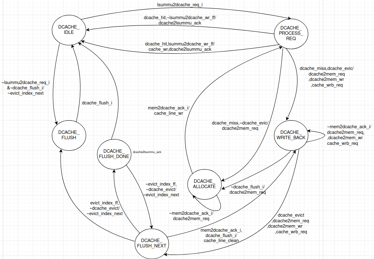
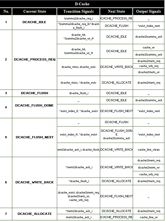
2.2.5. D-Cache
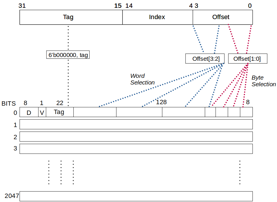
The Data Cache (DCache) is designed as a direct-mapped, write-back cache with byte-level accessibility, facilitated by the sel_byte signal. It comprises 2048 cache sets (DCACHE_SETS = 2048), which are indexed using 11 bits (DCACHE_INDEX_BITS = 11). Each cache line is 128 bits wide (DCACHE_LINE_WIDTH = 128), enabling efficient memory transactions and reducing latency for bulk data operations.
The cache operates within a 32-bit address space (DCACHE_ADDR_WIDTH = 32), in line with typical RISC-V system architectures. It supports 32-bit data words (DCACHE_DATA_WIDTH = 32), ensuring compatibility with standard word-based memory operations. The offset field spans 4 bits (DCACHE_OFFSET_BITS = 4), allowing fine-grained selection within a cache line, while the 17-bit tag field (DCACHE_TAG_BITS = 17) provides robust address mapping and cache line identification.
This configuration offers optimized memory access latency and efficient cache utilization, minimizing memory stalls and enhancing overall processor performance.
The structure of D-Cache in Pcore is shown as:
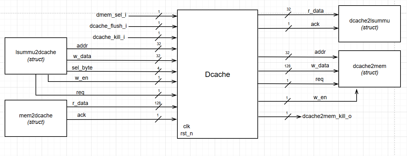
The top level diagram of D-Cache is given below:
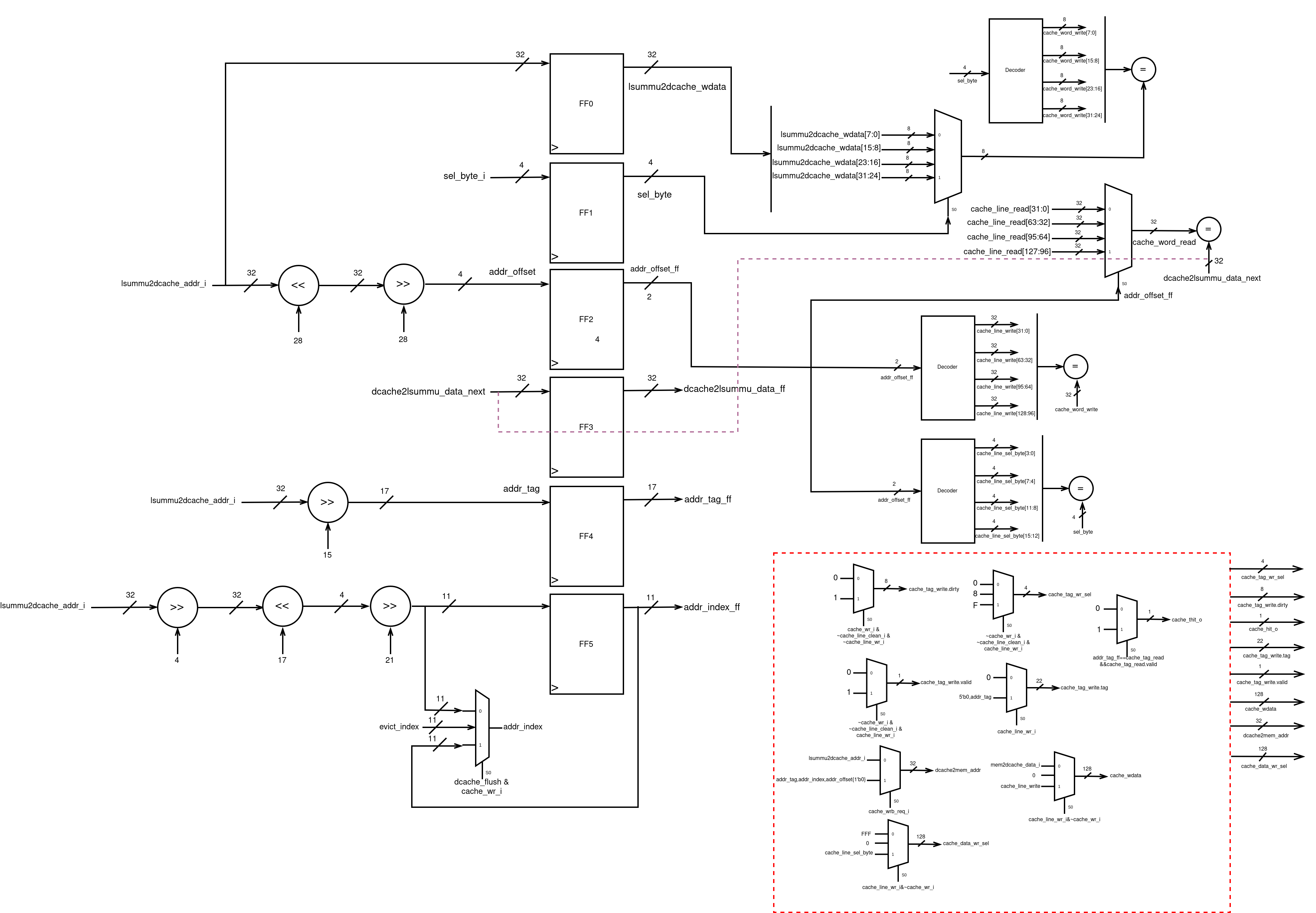
The datapath of Dcache is shown below:

The detailed datapath is shown below:
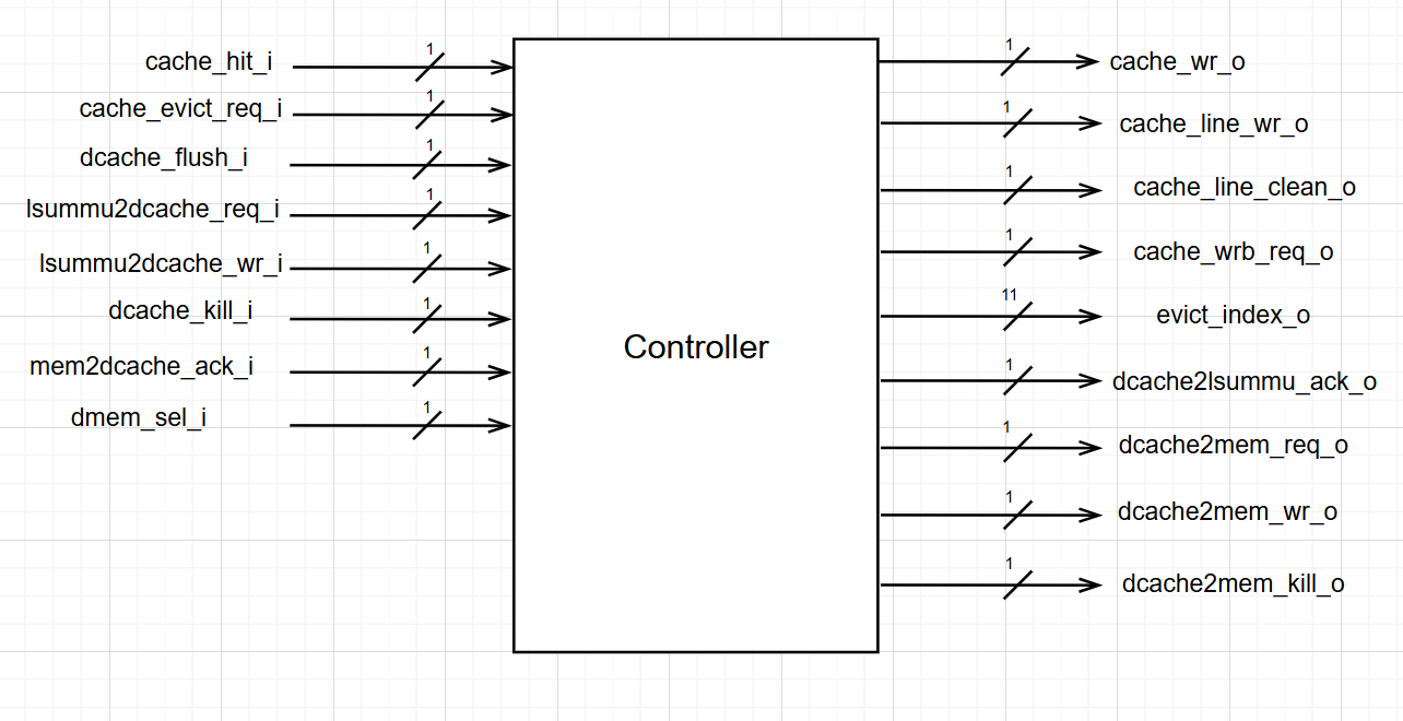
The controller of Dcache is shown as:
The state machine of Dcache is shown below:
The detailed table for state machine is given as:
2.2.6. I-Cache
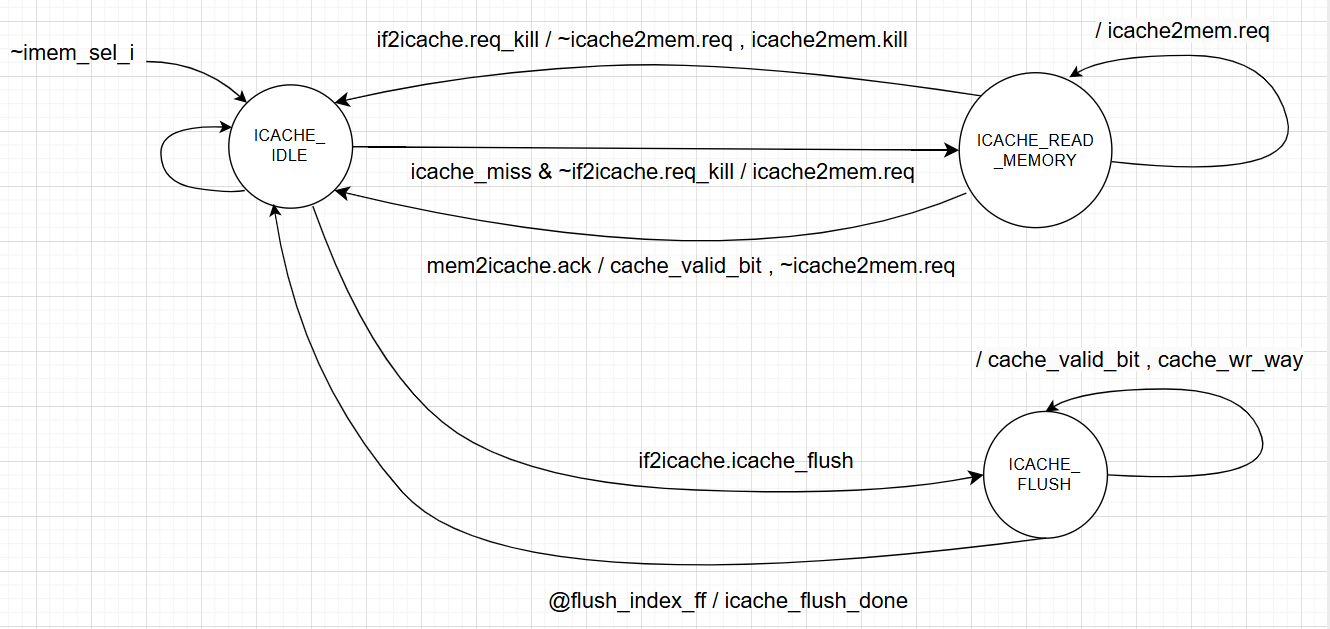
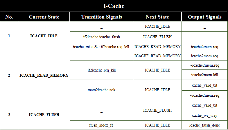
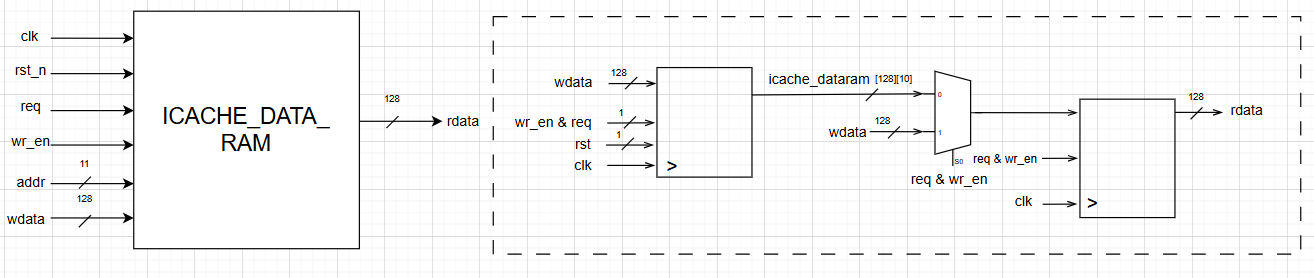
The I-cache of the Pcore is designed as a 4-way set-associative cache, where each set at a specific index holds four cache lines (or “ways”). Each way at a specific index contains a valid bit and a tag field to determine whether the data stored corresponds to the requested address. The cache uses a 32-bit address space (XLEN = 32), and the cache line width is 128 bits (16 bytes). There are 2048 sets in total, requiring 9 bits (ICACHE_IDX_BITS = 9) to index into the cache. Each cache line contains 16 bytes, so 4 bits (ICACHE_OFFSET_BITS = 4) are used to select the byte offset within the line. The remaining 22 bits (ICACHE_TAG_BITS = 22) form the tag used for cache lookup and comparison. The tag field begins at bit position 15 (ICACHE_TAG_LSB = 15) of the address. This organization allows efficient instruction fetches by enabling parallel tag comparisons across the 4 ways of a selected set, supporting both fast access and good spatial locality.
The structure of I-Cache in Pcore is shown as:

The top level diagram of I-Cache is given below:

The state machine of I-Cache is shown below:
The detailed table for state machine is given as:
Similarly, the diagram for I-Cache Dataram is given as:
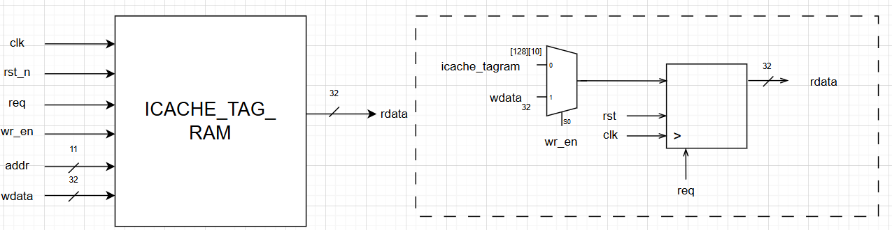
Similarly, the diagram for I-Cache Tagram is given as:
2.2.7. MMU Details
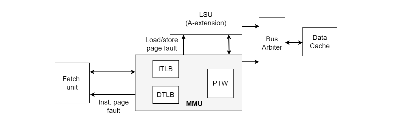
The memory management unit (MMU) is responsible for address translation when activated by configuring the corresponding CSR (i.e. satp register) and ensuring that the current privilege mode is lower than the machine mode. Enabling address translation also requires the ability to handle page faults. The MMU implements page-based 32-bit virtual-memory system conforming to Sv32 specifications. The MMU module interfaces with the LSU and fetch modules are shown in the accompanying figure below.
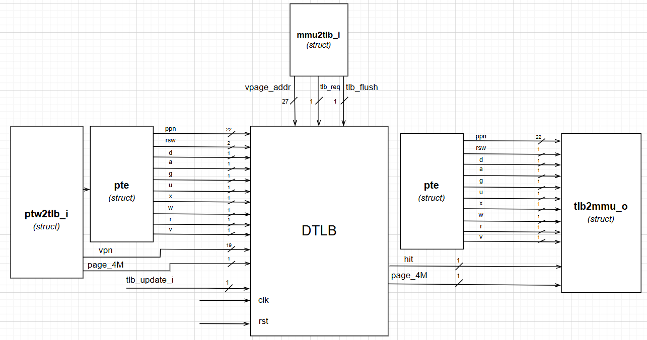
The MMU module implements separate TLBs for instruction and data memory interfaces along with a shared hardware page table walker (PTW). It is possible that we encounter both ITLB as well as DTLB misses during the same cycle.
The top level diagram of MMU is given below:

2.2.7.1. PTW
The hardware PTW arbitrates the address translation requests and prioritises DTLB miss over ITLB miss.
The top level diagram of PTW is given below:

The detailed datapath of PTW is shown below:

The state machine of PTW is shown below:

The detailed table for state machine is given as:

2.2.7.2. DTLB
The top level diagram of DTLB is given below:
2.2.7.3. ITLB
The top level diagram of ITLB is given below:

2.2.8. Booting and Peripherals
On processor reset, the first instruction executed depends on the PC reset value defined by the user configuration parameter PC_RESET defined in pcore_config_defs.svh in the rtl\defines. The default value of the parameter PC_RESET is 0x00001000, which is the starting address of the boot memory. The boot memroy is read only and is preinitialized with the zero-level boot loader (ZLBL). The ZLBL usually contains early system initializtions including some interface intialization required for loading either next level boot loader or user application. The boot memory can be accessed either from instruction or from data bus interface. Since boot memory is single port memory, a bus multiplexer is used to interface it with both instruction and data bus interfaces.
Curerntly the following peripherals are integrated with the processor core using the data bus interface. All these interfaces are non-cacheable and their address map is available in the SoC Memory Map subsection.
PLIC (platform level interrupt controller)
CLINT (core level interruptor)
UART
SPI